- 您现在的位置:买卖IC网 > Sheet目录1904 > ATF1502ASV-15JI44 (Atmel)IC CPLD EE HP 15NS 44-PLCC
16
1615J–PLD–01/06
ATF1502ASV
14. Power-down Mode
The ATF1502ASV includes an optional pin-controlled power-down feature. When this mode is
enabled, the PD pin acts as the power-down pin. When the PD pin is high, the device supply cur-
rent is reduced to less than 3 mA. During power-down, all output data and internal logic states
are latched and held. Therefore, all registered and combinatorial output data remain valid. Any
outputs that were in a high-Z state at the onset will remain at high-Z. During power-down, all
input signals except the power-down pin are blocked. Input and I/O hold latches remain active to
ensure that pins do not float to indeterminate levels, further reducing system power. The power-
down pin feature is enabled in the logic design file. Designs using the power-down pin may not
use the PD pin logic array input. However, all other PD pin macrocell resources may still be
used, including the buried feedback and foldback product term array inputs.
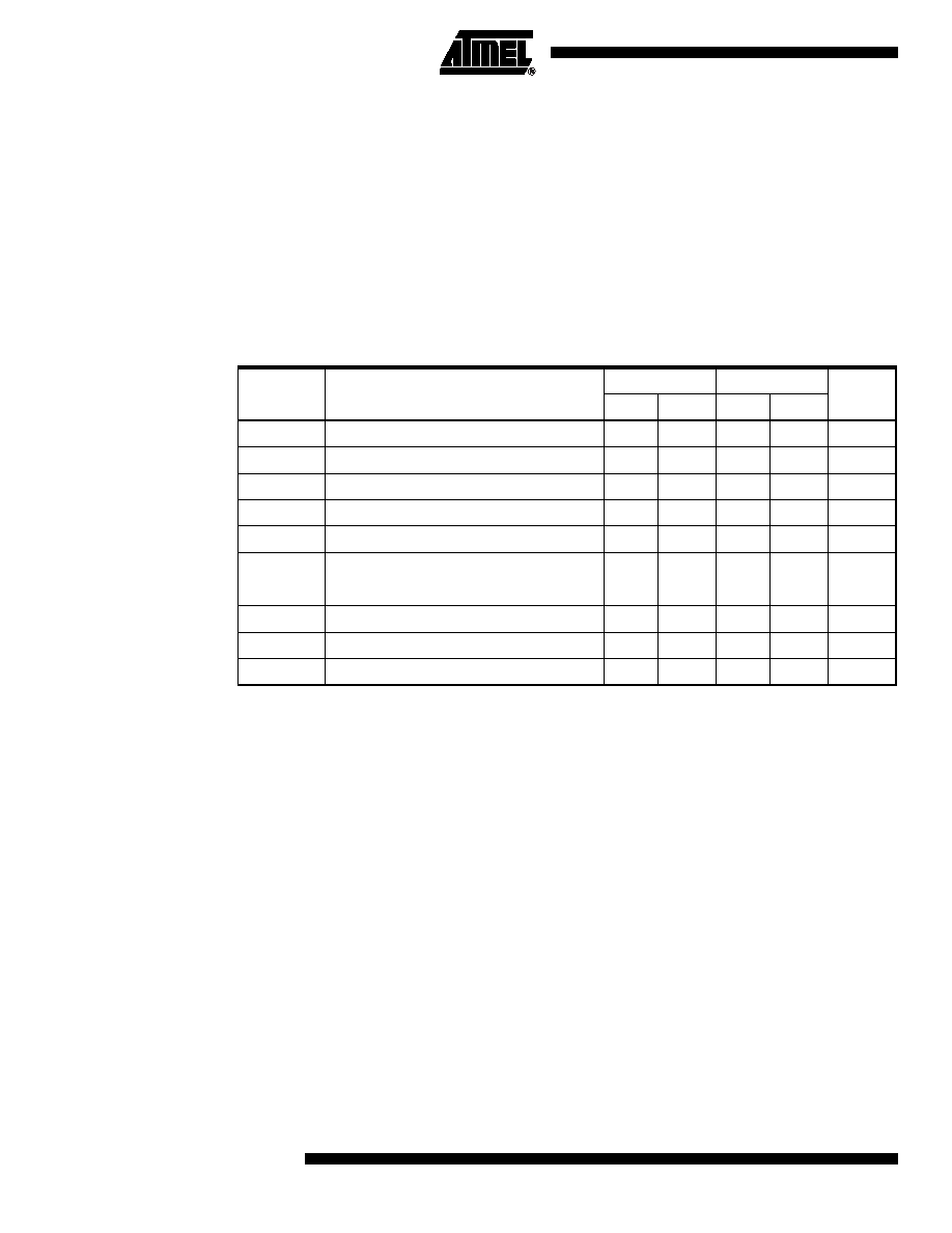
Notes:
1. For slow slew outputs, add t
SSO.
2. Pin or product term.
Table 14-1.
Power-down AC Characteristics(1)(2)
Symbol
Parameter
-15
-20
Units
Min
Max
Min
Max
tIVDH
Valid I, I/O before PD High
15
20
ns
t
GVDH
Valid OE(2) before PD High
15
20
ns
tCVDH
Valid Clock(2) before PD High
15
20
ns
tDHIX
I, I/O Don’t Care after PD High
25
30
ns
t
DHGX
OE(2) Don’t Care after PD High
25
30
ns
tDHCX
Clock(2) Don’t Care after PD High
25
30
ns
tDLIV
PD Low to Valid I, I/O
1
s
t
DLGV
PD Low to Valid OE(2)
11
s
tDLCV
PD Low to Valid Clock(2)
11
s
t
DLOV
PD Low to Valid Output
1
s
发布紧急采购,3分钟左右您将得到回复。
相关PDF资料
ATF1502BE-5AX44
IC CPLD 64MC 1.8V 44-TQFP
ATF1504ASVL-20QI100
IC CPLD 20NS LOWV LOWPWR 100QPFP
ATF1504BE-5AX100
IC CPLD 64MC 1.8V 100-TQFP
ATF1508ASL-25QI160
IC CPLD 25NS LOW PWR 160PQFP
ATF1508ASVL-20JU84
IC CPLD 20NS LOWV LOW PWR 84PLCC
ATF1508BE-5AX100
IC CPLD 128MC 1.8V ISP 100TQFP
ATF1508RE-5AX100
IC CPLD 128MC 3.3V ISP 100TQFP
ATF1508RE-7AU100
IC CPLD EE 128MC 5NS 100-TQFP
相关代理商/技术参数
ATF1502ASV-15JU44
功能描述:CPLD - 复杂可编程逻辑器件 CPLD 32 MACROCELL ISP STD PWR 3.3V RoHS:否 制造商:Lattice 系列: 存储类型:EEPROM 大电池数量:128 最大工作频率:333 MHz 延迟时间:2.7 ns 可编程输入/输出端数量:64 工作电源电压:3.3 V 最大工作温度:+ 90 C 最小工作温度:0 C 封装 / 箱体:TQFP-100
ATF1502ASV-20AC44
功能描述:CPLD - 复杂可编程逻辑器件 CPLD 32 MACROCELL ISP STD PWR 3.3V RoHS:否 制造商:Lattice 系列: 存储类型:EEPROM 大电池数量:128 最大工作频率:333 MHz 延迟时间:2.7 ns 可编程输入/输出端数量:64 工作电源电压:3.3 V 最大工作温度:+ 90 C 最小工作温度:0 C 封装 / 箱体:TQFP-100
ATF1502ASV-20AI44
功能描述:CPLD - 复杂可编程逻辑器件 CPLD 32 MACROCELL ISP STD PWR 3.3V RoHS:否 制造商:Lattice 系列: 存储类型:EEPROM 大电池数量:128 最大工作频率:333 MHz 延迟时间:2.7 ns 可编程输入/输出端数量:64 工作电源电压:3.3 V 最大工作温度:+ 90 C 最小工作温度:0 C 封装 / 箱体:TQFP-100
ATF1502ASV-20JC44
功能描述:CPLD - 复杂可编程逻辑器件 ASICS RoHS:否 制造商:Lattice 系列: 存储类型:EEPROM 大电池数量:128 最大工作频率:333 MHz 延迟时间:2.7 ns 可编程输入/输出端数量:64 工作电源电压:3.3 V 最大工作温度:+ 90 C 最小工作温度:0 C 封装 / 箱体:TQFP-100
ATF1502ASV-20JI44
功能描述:CPLD - 复杂可编程逻辑器件 ASICS RoHS:否 制造商:Lattice 系列: 存储类型:EEPROM 大电池数量:128 最大工作频率:333 MHz 延迟时间:2.7 ns 可编程输入/输出端数量:64 工作电源电压:3.3 V 最大工作温度:+ 90 C 最小工作温度:0 C 封装 / 箱体:TQFP-100
ATF1502ASVL-30AC44
功能描述:IC CPLD 32 MC 30NS EE 44TQFP 制造商:microchip technology 系列:ATF15xx 包装:托盘 零件状态:停產 可编程类型:系统内可编程(最少 10,000 次编程/擦除循环) 延迟时间 tpd(1)最大值:30.0ns 电源电压 - 内部:3 V ~ 3.6 V 宏单元数:32 I/O 数:32 工作温度:0°C ~ 70°C 安装类型:表面贴装 封装/外壳:44-TQFP 供应商器件封装:44-TQFP(10x10) 基本零件编号:ATF1502 标准包装:154
ATF1502ASVL-30JC44
功能描述:IC CPLD 32 MC 30NS EE 44PLCC 制造商:microchip technology 系列:ATF15xx 包装:托盘 零件状态:停產 可编程类型:系统内可编程(最少 10,000 次编程/擦除循环) 延迟时间 tpd(1)最大值:30.0ns 电源电压 - 内部:3 V ~ 3.6 V 宏单元数:32 I/O 数:32 工作温度:0°C ~ 70°C 安装类型:表面贴装 封装/外壳:44-LCC(J 形引线) 供应商器件封装:44-PLCC(16.59x16.59) 基本零件编号:ATF1502 标准包装:27
ATF1502BE
制造商:ATMEL 制造商全称:ATMEL Corporation 功能描述:Highperformance CPLD